Machining Parts for the Semiconductor Equipment Industry
The semiconductor industry is one of the most technologically advanced and rapidly evolving sectors in the world. It drives innovations in electronics, computing, communications, and artificial intelligence, making it a cornerstone of the modern digital economy. However, behind every chip fabricated in a cleanroom lies a vast ecosystem of specialized equipment, and at the foundation of that equipment are precision-machined parts.
Machining parts for semiconductor equipment is not the same as machining components for general industrial machinery. The demands are far more stringent, with requirements for ultra-high precision, tight tolerances, superior surface finishes, contamination control, and advanced material compatibility. The semiconductor industry depends on these qualities because even the slightest imperfection can compromise the performance of wafer fabrication, leading to yield losses worth millions of dollars.
This article provides a comprehensive look at the world of machining parts for semiconductor equipment. It explores the unique requirements of the industry, the materials and machining methods involved, the quality standards applied, and the future trends that continue to push machining technologies to new frontiers.
The Role of Machined Parts in Semiconductor Equipment
Semiconductor equipment is highly complex, often costing millions of dollars per machine. Within these machines are thousands of individual components, many of which must be custom-machined to exact specifications. Some critical areas where machined parts are used include:
- Wafer Handling Systems: Robots, end-effectors, and carriers require lightweight, precise, and contamination-free components.
- Vacuum Chambers: Machined aluminum, stainless steel, and exotic alloys are used to create ultra-clean environments for processes such as deposition and etching.
- Gas Delivery and Fluid Control Systems: Manifolds, fittings, and valves must be precision-machined to ensure leak-free operation.
- Lithography and Etching Equipment: High-precision stages and supports enable nanometer-level alignment during photolithography.
- Thermal Management Systems: Machined parts are essential for heat exchangers, cooling plates, and supports that ensure temperature stability.
So that machining plays a critical role in manufacturing components for semiconductor equipment, enabling the production of highly precise and reliable parts essential for chip fabrication. This involves using techniques like CNC machining, EDM, and laser machining to create components for various stages of semiconductor manufacturing, including lithography, etching, deposition, and inspection.
Unique Challenges of Machining for the Semiconductor Industry
Machining for semiconductor applications is distinct from general machining. The challenges include:
- Ultra-Tight Tolerances: Semiconductor components often require tolerances within ±1–2 microns.
- Surface Finish Requirements: Components must often achieve finishes better than Ra 0.2 μm, particularly for sealing and vacuum components.
- Contamination Control: Surfaces must be free of burrs, oils, and particulates that could compromise cleanroom conditions.
- Material Properties: Semiconductor equipment demands high-purity materials such as 6061-T6 aluminum, stainless steel 316L, Inconel, titanium, and ceramics.
- Complex Geometries: Many parts require 5-axis machining and advanced tooling to achieve undercuts, channels, and intricate shapes.
- High Production Costs: Due to the complexity and stringent standards, machining semiconductor parts involves higher costs than standard machining.
- Traceability and Documentation: Each part must be traceable, with detailed documentation of machining processes, materials, and quality tests.
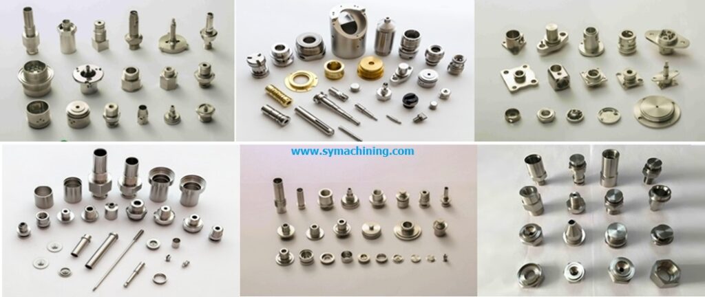
Materials Commonly Used in Semiconductor Equipment Machining
- Aluminum Alloys: 6061-T6 and 6061-T651, Widely used due to excellent machinability and strength-to-weight ratio.
- Stainless Steels: 316L Stainless Steel: Preferred for corrosion resistance and low contamination in vacuum environments. 304
- Stainless Steel: Used for structural parts that require strength and durability.
- Nickel-Based Alloys: Inconel 718 and Hastelloy, Withstand extreme heat and chemical environments, crucial for deposition chambers.
- Titanium Alloys: Grade 5 (Ti-6Al-4V): Offers high strength, corrosion resistance, and compatibility with harsh chemicals.
- Ceramics and Quartz: Alumina, Silicon Carbide, and Fused Quartz: Used for insulation, wear resistance, and plasma etching environments.
- Plastics and Composites: PEEK, PTFE, and Ultem: Applied in wafer handling and electrical insulation components.
Each material is chosen based on its mechanical properties, chemical resistance, and cleanliness, ensuring compatibility with semiconductor processing environments.
Precision Machining Processes Used
1. CNC Milling
Multi-axis CNC milling is used for complex components such as manifolds, cooling plates, and robotic parts.
2. CNC Turning
Produces cylindrical parts like fittings, connectors, and housings.
3. Grinding and Superfinishing
Used to achieve surface finishes in the nanometer range, essential for sealing components.
4. EDM (Electrical Discharge Machining)
Suitable for producing intricate shapes in hard materials, such as tungsten or ceramics.
5. Lapping and Polishing
Essential for wafer chucks and sealing surfaces that require ultra-smooth finishes.
6. Ultrasonic Machining
Applied in machining brittle materials like quartz and ceramics.
7. Additive and Hybrid Manufacturing
Increasingly used for rapid prototyping and specialized cooling channels in heat exchangers.
These processes must often be combined to achieve the precision, surface integrity, and cleanliness demanded by semiconductor equipment manufacturers.
Quality Control and Standards
Quality assurance is central to machining for semiconductor equipment. The following practices are standard:
- Metrology and Inspection
- Coordinate Measuring Machines (CMMs) for dimensional verification.
- Optical and laser scanners for surface profile inspection.
- Surface Cleanliness Testing
- Particle contamination analysis to ensure compliance with cleanroom standards.
- Vacuum Leak Testing
- Helium leak detection for vacuum chamber components.
- Material Certification
- Mill test reports (MTRs) to confirm chemical composition and mechanical properties.
- Industry Standards
ISO 9001, AS9100, and SEMI standards for semiconductor equipment manufacturing.
- Traceability
- Serialized part tracking for accountability and process control.
The level of quality control in semiconductor machining rivals that of aerospace and medical industries, ensuring zero-defect production.
Applications of Machined Parts in Semiconductor Equipment
- Wafer Fabrication Equipment
- Precision stages, chucks, and chambers.
- Testing and Inspection Equipment
- Fixtures, probe stations, and robotic handling systems.
- Deposition Equipment
- Vacuum chambers, gas manifolds, and electrode supports.
- Etching and Cleaning Equipment
- Plasma chambers, cooling blocks, and precision nozzles.
- Packaging Equipment
- Mechanical arms, precision molds, and bonding components.
- Every stage of semiconductor manufacturing relies on precision-machined parts to ensure efficiency, accuracy, and high yield.
Future Trends in Semiconductor Machining
- Nanometer-Level Machining
- As chips shrink below 3nm, machining tolerances will tighten even further.
- Advanced Materials
- Wider use of ceramics, composites, and new alloys for higher durability and chemical resistance.
- Automation and Smart Machining
- AI-driven CNC machines with real-time monitoring and adaptive control.
- Additive Manufacturing Integration
- Hybrid processes combining 3D printing with precision machining for complex cooling channels and lightweight structures.
- Sustainability
- Eco-friendly machining practices, recycling of scrap materials, and reduced use of harmful chemicals.
- Global Supply Chain Expansion
With increasing demand for chips, machining suppliers will expand globally, particularly in Asia and North America.
Choosing a trustworthy machining supplier
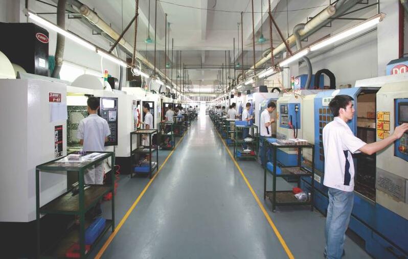
SYM precision machining specializes in machining services for over 25 years, our team has a good understanding of GD&T (geometric dimension & tolerance) to ensure tight tolerances. Also, we have advanced equipment for 5-axis, understanding fixture design for complex geometries. With rich experience and strict quality control, we can provide you with trustworthy service.
Conclusion
Machining parts for the semiconductor equipment industry represents the pinnacle of precision manufacturing. Unlike standard industrial machining, this field requires micron-level tolerances, flawless finishes, contamination-free processes, and robust documentation. Every wafer handler, vacuum chamber, manifold, and robotic arm in semiconductor fabs depends on the skill of machinists, the quality of materials, and the sophistication of machining technologies.
As the semiconductor industry continues to evolve—pushing towards smaller nodes, more complex architectures, and higher throughput—the role of precision machining will only grow in importance. Future innovations in machining technologies, material science, and automation will ensure that semiconductor equipment manufacturers can meet the ever-increasing demands of this critical industry.
Related article
PEEK Plastic CNC Machining Services | High-Performance Precision Parts